

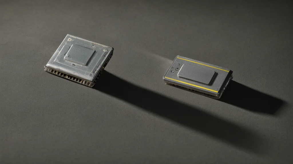
OpenAI's Jalapeño claims 3.6x lower latency than Nvidia's GB300 — but the numbers are independently unverified
The semiconductor race has for years been about one thing: who delivers the fastest accelerator. Two events within four weeks this autumn point to something else. On August 25, 2026, OpenAI fully revealed its first in-house AI accelerator, Jalapeño. On September 23, 2026, SiliconANGLE published an analysis based on conversations with technology leaders at AMD, Broadcom, Samsung and OpenAI, concluding that the competition is no longer about individual chips — but about entire systems. Together they mark a moment when custom accelerators, memory-centric design and LLM-assisted chip design become visible as a structural shift in the industry — not as isolated cases.
The thesis: the factory is the computer
It is worth being clear about what is what. The core thesis comes from John Furrier at SiliconANGLE, who writes that the discussion about AI infrastructure quickly becomes about systems: CPUs, GPUs and custom XPUs; memory and high-bandwidth memory; scale-up and scale-out networking; chiplets; advanced packaging; optics; cooling; software; electricity — and ultimately "entire campuses operating as massive computers." This is commentary and analysis, not established industry consensus. But it rests on statements from named leaders Furrier has interviewed over time: AMD CTO Mark Papermaster, Broadcom's semiconductor chief Charlie Kawwas, Samsung's Paul Cho and OpenAI's hardware lead Richard Ho.
The point is concrete: when an AI datacenter operator builds out capacity, performance is no longer determined by the individual GPU. It is determined by how quickly data moves between compute chips and memory, how chips are packaged together, how racks are connected with copper and optics, how much power and cooling the campus can support, and how the software exploits all of it. Co-designing all of these layers around a known workload is the new competitive arena — if the thesis holds.
Three positions from industry leaders
The four leaders Furrier cites do not paint a unified picture, and that is precisely what makes the material useful. They represent three different positions within the same shift.
Kawwas: XPUs are a niche for the few. Broadcom's semiconductor chief, according to SiliconANGLE, framed custom accelerators as a market genuinely available only to a relatively small number of frontier AI companies operating at enormous scale — with enough ownership of the software stack and predictable demand to amortize development costs. Google, AWS, Microsoft, Meta and OpenAI all have internal accelerator programs. That is an important caveat: the system shift does not mean everyone can or should build their own chips.
Cho: Memory is the design center. Samsung's Paul Cho described the shift concisely, according to SiliconANGLE: "Memory is no longer a supporting player in AI infrastructure — it is becoming the design center." The background is that data movement — bandwidth, capacity, power and proximity to compute — increasingly determines performance. It also explains why the memory vendors' position has strengthened: when an accelerator is largely defined by how much HBM it can address, and how fast, power partially shifts from the compute chip to the memory stack around it. It should be noted that Cho is quoted via SiliconANGLE; the exact timing and occasion of the statement are not specified in the reporting.
Papermaster: The general-purpose chips endure. AMD's CTO argued that broad-coverage CPUs and GPUs are not going away. Instead, modular architectures and chiplets let semiconductor vendors create workload-specific variants — including configurations for agentic workloads — on common platforms. That is the counterpoint: system thinking does not have to mean every customer designs its own silicon from scratch.
Jalapeño as a test case
OpenAI's Jalapeño is the most concrete example of what "whole-system" competition means in practice — and at the same time a reminder of what has not yet been proven.
The chip was fully revealed on August 25, 2026 as the company's first AI accelerator. It delivers up to 13.4 petaflops of compute in 4-bit precision and addresses 232 GB of the most advanced memory type available, connected at 15.4 terabytes per second. Benchmarks OpenAI itself cites claim up to 3.6x lower end-to-end latency than Nvidia's GB300, at lower power.
That last point requires precision: these figures are the company's own benchmark results, not independently verified measurements. IEEE Spectrum explicitly notes that it remains to be seen whether the numbers translate into real gains when Jalapeño is deployed at scale in OpenAI's inference fleet. Until then, 3.6x is a claim, not a fact.
What is well documented, however, is the design philosophy. Richard Ho, vice president of hardware at OpenAI, said according to SiliconANGLE that Jalapeño is optimized around the "kernels, memory movement, networking and serving patterns" that matter for frontier models. It is the system thesis in miniature: the chip is not designed to win a general-purpose benchmark, but to fit a specific, internally known workload pattern.
Under 20 months — and why
Perhaps the most debated figure is the timeline. Jalapeño went from first architectural concept to first silicon in under 20 months. Only nine months separated first RTL — the register-transfer-level code that defines the chip's logic — from tape-out, when the finished design is sent to production. The design team averaged fewer than 100 people, around 100 today, and OpenAI partnered with Broadcom on physical design.
Part of the explanation lies in the toolchain. OpenAI built its front-end workflow around Accelerated Hardware Synthesis (XLS), an open-source high-level synthesis toolchain originally developed at Google. Chris Leary, a member of OpenAI's technical staff, explains why LLMs worked well here: "XLS looks like software in many ways, so it got that advantage." Ho puts the point even more bluntly: "The models give our engineers superpowers."
But it would be wrong to attribute the speed to LLMs alone — and independent experts make exactly that point. David Chin, co-founder of the chip design company Verkor.io, says the "timeline they gave us is quite credible," but believes Broadcom's help was crucial to Jalapeño's rapid timeline. Andrew Kahng at UC San Diego called the timeline "likely best in class today." In other words: the credibility is underscored, but the causal explanation is two-part — LLM-assisted front-end work on top of a highly experienced physical design partner with mature infrastructure.
That does not mean the LLM contribution is insignificant. It means "under 20 months" cannot be straightforwardly generalized to "LLMs revolutionized chip design." Team size, the partnership and the tool choices are intertwined, and it remains to be seen how much of the method can be replicated by companies without a Broadcom tract.
Who can actually afford this?
Kawwas' caveat deserves its own weight. Own silicon, by the logic he lays out, requires three things simultaneously: operating at a scale where even small efficiency gains pay off the development costs, ownership of the software stack the chip is optimized against, and predictable demand enough to plan a production fleet. That is why the list of players with internal accelerator programs is so short: Google, AWS, Microsoft, Meta and OpenAI. All are simultaneously large customers of commercial accelerators — own silicon, in this reading, is a bargaining lever and a bottleneck-reducer, not necessarily a replacement.
For everyone else — second-tier cloud providers, enterprise customers, the public sector — the system shift means something different: they are price- and architecture-takers in a market where the terms of competition have become harder to compare. A chip optimized for one player's inference patterns is not directly comparable to a general-purpose GPU on a price-per-flop list, and that is partly the point.
What remains open
Two big questions are unanswered in the evidence. The first is whether Jalapeño's benchmark figures hold up in production. IEEE Spectrum is explicit that real gains in OpenAI's inference fleet remain to be seen; no independent measurement of the latency or power advantage over the GB300 exists. The second is whether the system shift applies beyond the few frontier players. The positions of Kawwas, Cho and Papermaster can be read as three answers to the same question — niche, center, platform — but who is proven right will be determined by something none of them can promise today: how quickly workloads stabilize, and how cheaply modular platforms can be adapted.
The documented record is nonetheless enough to establish the direction. Memory has been elevated from supporting role to design center. Networking, packaging, cooling and power are co-design objects, not afterthoughts. And a chip designed around its own workloads, in under 20 months and with a team of fewer than 100, shows that the entry ticket to own silicon has gotten lower — even though it remains high enough that only a few can pay it.
(Sources: SiliconANGLE, September 23, 2026, IEEE Spectrum)