

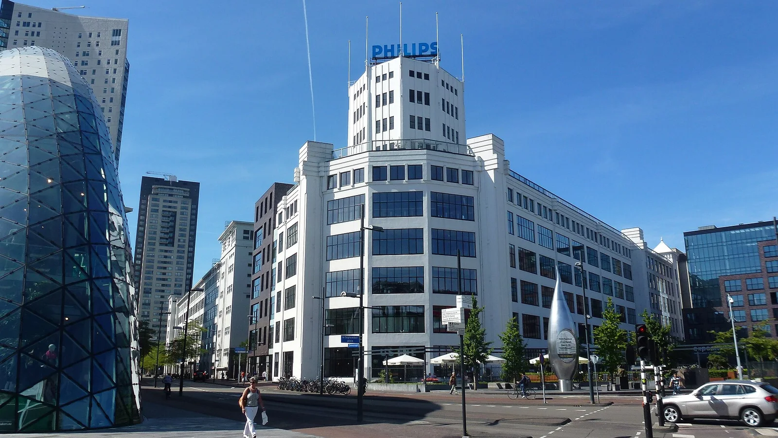

TNO is building a 10,000-square-metre facility for six-inch photonic wafer production in Eindhoven
Europe's photonic chip initiative PIX Europe has been pledged €400 million by the EU, while the Dutch research organisation TNO is already building a 10,000-square-metre pilot line facility in Eindhoven.
The European photonic chip initiative PIX Europe has been pledged €400 million by the EU, while the Dutch organisation TNO is already building a 10,000-square-metre pilot line facility in Eindhoven. The initiative comes down to one technical leap: scaling photonic chip production from four-inch to six-inch wafers — and all of it rests on BBC reporting, not independent confirmation.
The news: €400 million for PIX Europe
The European Union has committed €400 million ($450 million; £330 million) to a project called PIX Europe, which, according to the project's own description, is to make the continent "a global leader in new technology for photonic chips". The figure and the goal are as reported by the BBC, and there are so far no primary sources — such as a European Commission press release — confirming the amount or the project's purpose.
What are photonic chips?
Photonic chips use light instead of electricity to perform computations and transfer data. Because light rather than electrons does the work, the chip is faster, uses less energy and generates less heat than traditional electronic chips. The BBC presents this as a general technical characteristic — these are not claims that photonic chips can replace electronic chips in general, only that the three properties are real advantages where they apply.
The facility: 10,000 square metres on the High Tech Campus
TNO — the Netherlands Organisation for Applied Scientific Research — is already building a 10,000-square-metre facility on the High Tech Campus in Eindhoven to produce six-inch indium phosphide wafers. According to Ton van Mol, who leads the work at TNO, the facility is to be fully opened in 2030, and he describes it as an important step not only for European but for global photonics.
Why six inches matters
Van Mol explains it this way: "Production of photonic chips globally is done today on wafers that are four inches (10 cm), and the next step is to scale production up to a six-inch wafer." The scale upgrade from four to six inches is the technically decisive step: more chips per wafer means lower cost per chip, but requires that the process be kept stable and reproducible.
The target for 2030, according to van Mol: "In 2030 we hope that we have a stable, reproducible process with high yield, and then the intention is that the pilot line is opened up to industrial parties who can turn it into commercial production." In other words, first prove that the process works predictably at scale, then let industrial players in.
The framework: the EU Chips Act and the pilot lines
Van Mol ties the programme to the European Chips Act: "the European Chips Act was then brought to life, and part of the law is to build pilot lines that really bring the technology, which is now in laboratories, to the next stage — production." The pilot lines are thus intended as a bridge between research and industrial production, and the Eindhoven facility is one concrete example of this model.
Perspective: ASML and Wennink's market forecast
Stanislas Baron, head of ASML's EU/US Customer Team, points to what he sees as Europe's core challenge: "Europe has a strong position in photonic research. The next challenge is to translate these innovations into industrial-scale production." According to the BBC, products from ASML — which supplies chipmaking equipment globally — will sit at the heart of the Eindhoven pilot line.
The former ASML chief executive Peter Wennink has been a vocal supporter of the Eindhoven project. He is the author of an influential report for the Dutch government called The Roadmap to Future Prosperity, which, according to the BBC's account, pointed to the photonic market being expected to grow 10 to 20 times over the next decade. This is the report's forecast, not a verified fact — and it is worth treating as an interested party's statement about a market he wants to succeed.
Open questions
Everything in this story rests on a single BBC article and quotes from parties with a stake in the initiative: TNO leads the facility, ASML supplies equipment to it, and Wennink wrote the report that argues for it. There is no independent confirmation of the €400 million figure, the timeline or the market forecast from the European Commission, from TNO itself or from the Dutch authorities in the form of primary documents.
It is also unclear how the €400 million is to be distributed, which partners are part of PIX Europe beyond TNO, and what production volumes the facility is aiming at — details the source material does not cover. Whether photonic chips will actually grow into a tenfold or twentyfold market by the 2030s is a forecast that can only be answered in hindsight.
Note: The BBC article's publication date is unconfirmed; the source states only its relative age at the time of retrieval.